Defects play an important role in the electronic properties of materials. In 2D materials, defect engineering has been used to impart exciting properties to the host material that are finding application in catalysis, nanoelectronics, sensing, quantum sciences and beyond.
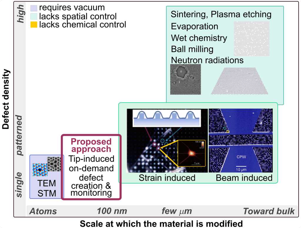
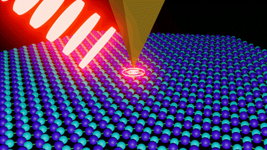
Our group has investigated the role of various defect engineering techniques on the properties of 2D materials. Our most recent work focuses on nanoscale defects that can be created using various functionalities of atomic force microscopy (AFM).
Our current work aims to expand our AFM-based defect engineering methods to:
- controllably create sub-50 nm defect with different composition and functionalities
- pattern the defects to understand the effect of expanding lattice distortion on the properties of the material
- design 2D material-based devices with targeted applications in sensing and catalysis
- use the experimental platform to complement the development of machine-learning-driven theoretical modeling that will accelerate the development of novel materials
Our work to data encompasses the evaluation of how defects impact properties of 2D materials at different scales:
- Defects in hexagonal boron nitride (h-BN) has led to the discovery of new catalytic processes
- Interaction of 2D materials with top-layers has led to the tuning of their photoluminescence
- Treatment of 2D materials with oxygen plasma has led to the tuning of their bandgap
Related publications
- F.E. Torres-Davila, M. Molinari, R.G. Blair, N. Rochdi, L. Tetard, Enhancing Infrared Light–Matter Interaction for Deterministic and Tunable Nanomachining of Hexagonal Boron Nitride, NanoLetters, doi.org/10.1021/acs.nanolett.2c02841, 2022
- F.A. Chowdhury, B. Pradhan, Y. Ding, A. Towers, A. Gesquiere, L. Tetard, J. Thomas, Perovskite quantum dot-reduced graphene oxide superstructure for efficient photodetection, ACS Applied Materials and Interfaces, 12(40), 45165-45173, 2020
- B. Pradhan, S. Das, J. Li, F. Chowdhury, J. Cherusseri, D. Pandey, D. Dev, A. Krishnaprasad, E. Barrios, A. Towers, A. Gesquiere, L. Tetard, T. Roy, J. Thomas, Science Advances, 6 (7), eaay5225, 2020
- Y. Ding, F. Torres Davila, A. Khater, D. Nash, R. Blair, and L. Tetard, Defect engineering in Boron Nitride for catalysis, MRS Communication, 8(3), 1236-1243, 2018
- A. Safaei, J. Calderon, D. Franklin, A. Vazquez-Guardado, L. Tetard, L. Zhai, M. N. Leuenberger, D. Chanda, Dynamically tunable extraordinary light absorption in monolayer graphene, Physical Review B, 96(16), 165431, 2017
- N. Choudhary, M.R. Islam, N. Kang, L. Tetard, Y. Jung, S.I. Khondaker, Two-dimensional lateral heterojunction through bandgap engineering of MoS2 via oxygen plasma, Journal of Physics: Condensed Matter, 28 (36), 364002, 2016
- N. Kang, H. P. Paudel, M. N. Leuenberger, L. Tetard, S. I. Khondaker, Photoluminescence Quenching in Single-Layer MoS2 via Oxygen Plasma Treatment, The Journal of Physical Chemistry C, 118 (36), 21258-21263, 2014
- U. Bhanu, M. R. Islam, L. Tetard and S. Khondaker, Photoluminescence quenching in gold-MoS2 hybrid nanoflakes, Scientific Reports, 4, 5575, 2014
- M. R. Islam, N. Kang, U. Bhanu, H. P. Paudel, M. Erementchouk, L. Tetard, M. N. Leuenberger, S. I. Khondaker, Tuning the electrical property via defect engineering of single layer MoS2 by oxygen plasma, Nanoscale, 6 (17), 10033-10039, 2014
Related patents
- L.Tetard, R. Blair, Low Temperature Photochemical Patterning of Carbon Nano- And Microstructures, Docket No UCF 2022-053-01 / 1513001.133US0, 2022
- L.Tetard, Controlled Creation of Sub-50 nm Defects in 2D Materials at Low Temperature, Docket No 2022-054-01 / 1513001.134US0, 2022
- F. E. Torres-Davila, R. G. Blair, L.Tetard, Photochemical transformation using engineered metal-free hexagonal boron nitride, USAN 17/859,550 filed July 7, 2022; Claims priority to USAN 63/219,333 filed July 7, 2021, and USAN 63/352,2793 filed June 16, 2022
- M. R. Islam, L.Tetard, S. I. Khondaker, Plasma treated semiconductor dichalcogenide materials and devices, US Patent 20,150,294,87, 2016