Condensed-matter physics (CMP) deals with the properties of matter in either a solid or liquid state. The approach taken is to apply fundamental physical laws obtained from quantum mechanics, electrodynamics, and thermodynamics to the description of matter in condensed phases. Many potential technological applications have emerged from fundamental CMP research, including semiconductor electronics and lasers, plasmonics, medical imaging, and magnetic and optical storage systems.
The research interests CMP groups in the UCF physics department span a wide range of areas, including topological Dirac materials, two-dimensional materials, surface science, superconductivity, semiconductor physics, nanomagnetism, nanotransport, nanocatalysis, energy-related materials. Several CMP faculty members are active users of national and international laborites including the Advanced Light Source (ALS) at Lawrence Berkeley National Laboratory, Stanford Synchrotron Radiation Lightsource (SSRL) at SLAC, National Synchrotron Light Source (NSLS) at Brookhaven National Laboratory, Swiss Light Source at Paul Sherrer Institute, Switzerland, Hiroshima Synchrotron Radiation Center, Japan, and the National High Magnetic Field Laboratory (NHMFL-Tallahassee). The research conducted by the UCF CMP group will potentially lead to exciting novel applications and advancements in emerging technologies.
Dr. Enrique Del Barco group:
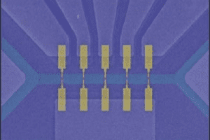
Del Barco’s group has ample experience in the study of nanoscale magnetic materials in a broad range of physical conditions, and with different experimental characterization techniques (e.g., high-sensitivity micro-Hall effect and SQUID magnetometry, high-frequency EPR and FMR spectroscopy, and single-electron transport spectroscopy). Del Barco has been a leading participant in the development of the field of single-moleculemagnets, having made seminal contributions, including the first proposal to employ molecular magnets in quantum computation. Del Barco’s group is also actively involved in the realm of spintronics, being co-author of an influential article on precessional switching of spin transfer torque (STT) nanoscale devices, which are now at the verge of mass commercialization as fast/low-energy-consumption MRAM. More recently, del Barco’s group has focused on charge/spin transport studies in low-dimensional systems, including graphene, and single-electron transport measurements through individual molecules.
Dr. Lee Chow group:
: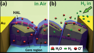
Professor Lee Chow studies the synthesis and fabrication of nanosensors based on oxide semiconductors. He also studies the dopants distribution as a function of annealing temperature in nano-crystalline thin films.
Dr. Leonid Chernyak group:
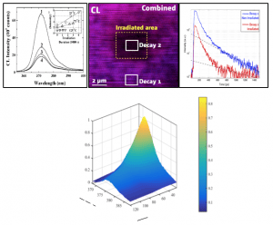
It has been discovered that electron injection into GaN (ZnO; Ga2O3) by either electron beam or forward-bias in the solid-state results in significantly longer lifetime of minority carriers, which is translated into suppressed photo-generated carrier recombination (top left figure), longer minority carrier diffusion length (due to increased carrier lifetime) and, therefore, enhanced photoresponse from GaN (ZnO) photovoltaic detectors. Top left figure demonstrates light emission (cathodoluminescence (CL)) decay observed in p-GaN subjected to electron beam
irradiation up to 4000 seconds at room temperature. The inset of the same figure shows variable-temperature dependence of intensity on duration of electron irradiation. These results are consistent with combined monochromatic image (top center figure) (band edge (350-390 nm) and defect emission (514-614 nm) of GaN with two areas under test (non-irradiated (Decay 1) and irradiated (Decay 2)) as well as with unique time-resolved CL (TR CL) measurements in top right figure, which shows TR CL decays from the areas under test. CL time decay is proportional to the inverse slope of the linear fit. More gradual slope for the irradiated area indicates larger non-equilibrium carrier lifetime in it, as compared to the non-irradiated one. Longer lifetime translates into suppressed CL (compare red and blue spectra) and larger carrier diffusion length, which has significant device applications. Material temperature is another factor, which affects non-equilibrium carrier dynamics in wide band gap semiconductors. The relevant results are shown in bottom three-dimensional plot.
Dr. Madhab Neupane group:
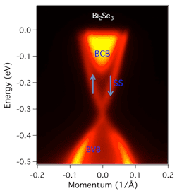
The Experimental Condensed Matter Physics group at UCF led by Dr. Madhab Neupane focuses on the investigation of emergent quantum materials such as topological insulators as well as Dirac, Weyl, and nodal-line semimetals. Topological insulators (TIs) are new quantum phases of matter characterized by an insulating bulk state and gapless spin-polarized linearly dispersive (Dirac like) surface states. The three-dimensional (3D) Dirac, Weyl, and nodal-line semimetals are a new class of materials, which are analogous to graphene with linearly dispersing bands that can host exotic new quantum states. Dr. Neupane’s group focuses on discovery and understanding of these new quantum materials using spectroscopic techniques. In particular, he utilizes angle-, spin- and time-resolved spectroscopic probes to reveal the interesting electronic and spin properties as well as the momentum resolved dynamical properties (light-matter interactions) of the bulk and symmetry-protected surface associated with these quantum materials. A number of novel electronic properties of these new quantum materials promise innovative technological applications in the fields of quantum computing, spintronics, low-powered electronics, plasmonics, and THz technology.
Dr. Masa Ishigami group:
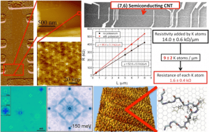
A single atomic scale defect or adsorbate has the ability to drastically influence properties of nanoscale materials. My laboratory has developed and utilized a wide array of experimental techniques to establish absolute control of experimental environments down to the atomic scale in order to measure the intrinsic properties of materials such as carbon nanotubes and graphene, a single layer of graphite. Our unique approach allows for exploration of a wide range of material properties beyond the reach of others. To date, we have resolved atomic structures of graphene and nanotube devices, demonstrated the impact of adsorbed atoms on transport properties of graphene, measured friction of gold nanocrystals at ultra high surface speeds, determined structure of oligopeptides on graphene and identified the dominant native scatterers in graphene. We hold a patent on a novel spectrometer technology and my results have played a large role in establishing nanoscale sensor technologies based on nanotubes and graphene.
Dr. Mihai Vaida group:
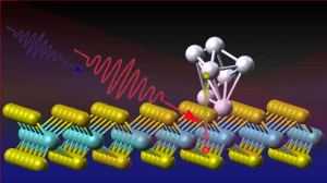
The research group of Dr. Vaida uses a state-of-the-art femtosecond laser system in conjunction with a high harmonics generation source and a monochromator to produce femtosecond laser pulses in the extreme ultraviolet spectral range. These laser pulses are employed to track the charge carrier dynamics in novel 2D nanostructured materials with time resolution, surface sensitivity, and element specificity. Moreover, pump-probe femtosecond laser mass spectrometry technique in conjunction with extreme ultraviolet soft ionization at the surface is used to study the ultrafast dynamics of molecules attached at solid surfaces such as bond breaking and bond making, with time‑, mass-, and energy-resolution. The main goal of this research is to fully monitor and understand the electron and molecular dynamics at the surface of various nanostructured materials that can be used to construct highly efficient photocatalytic and photovoltaic devices.
Dr. Paulo Eduardo de Faria Junior group:
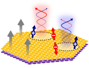
Dr. Faria’s research group covers a broad range of topics in theoretical condensed matter physics with a strong overlap with materials science. The group employs and develops novel computational approaches based on first principles (ab initio) methodologies, effective Hamiltonians, and group theory analysis to study the fundamental aspects and potential applications of various quantum materials in the field of optoelectronics, optospintronics, and quantum information technology.
Dr. Richard Klemm group:
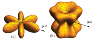
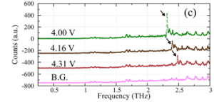
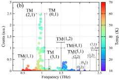
The Klemm research group is currently interested in p-wave superconductivity, the Knight shift in metals and superconductors, a quantum particle in high-symmetry two-and three-dimensional boxes, the coherent terahertz emission from the high-temperature superconductor Bi2Sr2CaCu2O8+ (BSCCO), and more generally the orbital symmetry of the superconducting order parameter in unconventional superconductors.
We are also engaged in studies of a quantum particle in high-symmetry disk, square, equilateral triangular, and cubic boxes, in which a single particle is confined due to the infinite potential outside the box. For the similar high-symmetry thin BSCCO microstrip antennas, only the wave functions that are one-dimensional representations of the appropriate point group are fixed in orientation over several periods of the ac Josephson current source, so the only cavity modes that can be excited arise from these wave functions. See Fig. 1. Experimental results from a thermally-managed BSCCO disk microstrip antenna are also shown in Fig. 1, indicating that the transverse magnetic (1,1) mode due to a two-dimensional group representation is missing, and also that the linewidth at the 2.4 THz emission frequency is very narrow, placing a lower limit of 9.8 meV on the bulk superconducting gap of BSCCO.
Dr. Saiful Khondaker group:
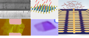
Professor Saiful Khondaker’s Nanophysics and Nanoelectronics group is interested in the fabrication and electron transport properties investigation of nanoscale electronic devices. Of particular interests are growth, assembly, and tailoring of the electrical and optical properties of the nanomaterials through doping, interface and defects engineering. Fabrication of prototype functional devices, and systems that exploit these new properties are also a focus. Current areas or interests are two dimensional materials and heterojunctions, carbon nanotubes, graphene and organic semiconductors.
Dr. William Kaden group:
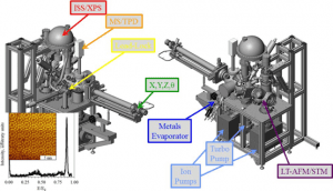
The Kaden group specializes in applying ultrahigh-vacuum (UHV, c.a. 10 TRILLION-fold lower pressure than your current ambient environment) surface-science methodologies to elucidate and thoroughly investigate the most fundamental physical driving forces governing catalytic processes at the interface of “model” catalytic systems. Put more specifically, the primary aim of the group is to draw upon directly attainable atomic- and molecular-level experimental data to more fully understand elementary structural-electronic-chemical relationships relevant to targeted reactions of interest at the interfaces of catalytic materials ranging from two-dimensional thin-films and supported clusters created within UHV to powders produced via industrially compatible wet-chemical techniques. UHV techniques housed within our surface-science apparatus include: Scanning Tunneling Microscopy/Spectroscopy, Atomic Force Microscopy/Spectroscopy, Low Energy Electron Diffraction, Xray Photoemission Spectroscopy, Ion Scattering Spectroscopy, and Mass Spectroscopy/Temperature Programmed Desorption.
Dr. Xiaofeng Feng group:
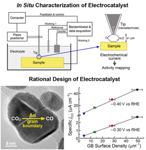
Our research is focused on rational design of nanostructure d materials for electrocatalytic energy conversion. Electrocatalysis plays a key role in energy conversion processes that are central to renewable energy technologies such as fuel cells and electrolyzers. In most cases, poor catalyst performance is the major source of efficiency loss for the entire device. For example, fuel cells are promising for direct conversion of chemical energy to electricity, but current devices suffer from efficiency losses caused by the poor catalytic performance of cathode materials in reducing oxygen. To find highly active and stable electrocatalysts, we need to establish design principles based on our understanding of structure–activity relationships. We will use in situ scanning probe microscopy and synchrotron-based X-ray spectroscopy to probe the catalyst interface and reveal new active sites and reaction intermediates. The understandings will be used to guide the design and synthesis of electrocatalysts (metal nanostructures, 2D materials) for fuel cells and artificial photosynthesis. Various synthesis methods such as vapor deposition, electrodeposition, and colloidal synthesis will be tailored to prepare catalytic materials with desired features, which will be characterized using different techniques (SEM, TEM, XRD, XPS, etc.).
Dr. Yasuyuki Nakajima group:
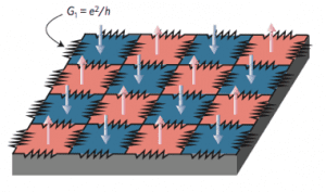
This group’s research focuses on design, discovery, synthesis and characterization of novel functional quantum materials, including unconventional superconductors, topological insulators/semimetals, and strongly correlated electron systems. In particular, the group is interested in searching for novel exotic phases of matter emerged in quantum materials in the presence of the combination of symmetry breaking, topological order, and strong electron correlations. To explore the novel electronic phases of matter, the group utilizes sophisticated characterization techniques, such as charge/thermal transport and thermodynamic measurements in the millikelvin range.
